


The growth of thin films via chemical vapor deposition (CVD) is an industrially significant process with a wide array of applications, notably in microelectronic device fabrication. CVD is carried out by passing a volatilized precursor (such as a silane, organometallic, or metal coordination complex) over a heated substrate. Thermal decomposition of the precursor produces a thin-film deposit, and the ligands associated with the precursor are cleanly lost to the gas phase as reaction products. Compared to other thin-film production techniques, CVD offers several significant advantages, most notably the potential for selective deposition and lower processing temperatures. Many metal CVD depositions are autocatalytic. Growth of such thin films is characterized by an induction period, which is a consequence of the higher barriers that relate to the activation of the precursor on a non-native substrate.
Benefits of the ALD method compared to the other methods are film uniformity, precise thickness control, excellent step coverage, and high reproducibility. Films can even be deposited routinely even onto curved substrates.
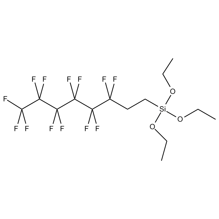
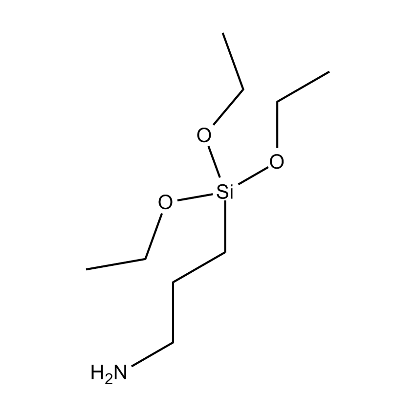
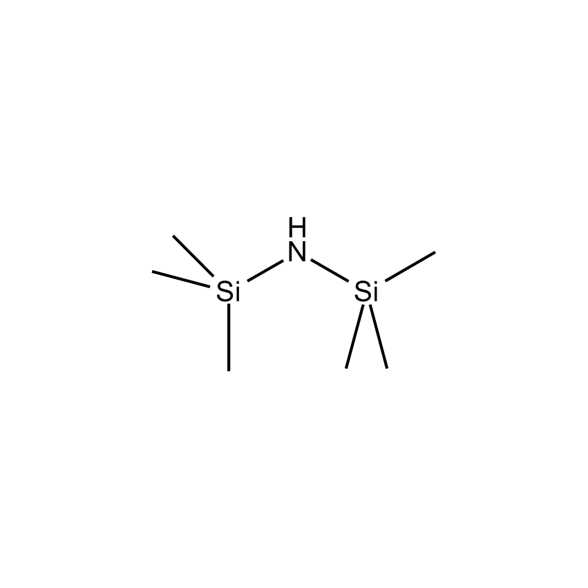
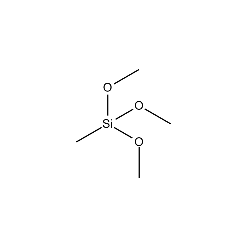
Silanes can be applied to substrates under dry aprotic conditions by CVD, which favors monolayer deposition. Although under proper conditions almost all silanes can be applied to substrates in the vapor phase, those with vapor pressure >5 torr at 100 °C have achieved the greatest number of commercial applications. In closed chamber designs, substrates are supported above or adjacent to a silane reservoir and the reservoir is heated to achieve 5 mm vapor pressure. Alternatively, vacuum can be applied until silane evaporation is seen. The silane can also be prepared in toluene solution, which when refluxed allows sufficient silane to vaporize through its inherent partial pressure. Here, the substrate temperature should be maintained between 50-120 °C to promote reaction. Cyclic azasilanes deposit the quickest (usually <5 mins). Amine-functional silanes also deposit rapidly (~30 mins) without a catalyst. Other silanes require extended reaction times, usually 4-24 hours. Such silane reactions can be promoted by adding catalytic amounts of amines.
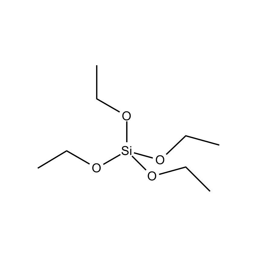
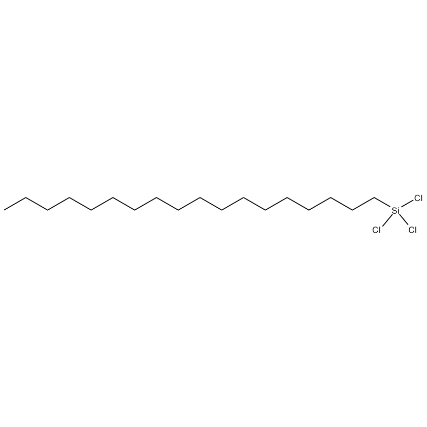
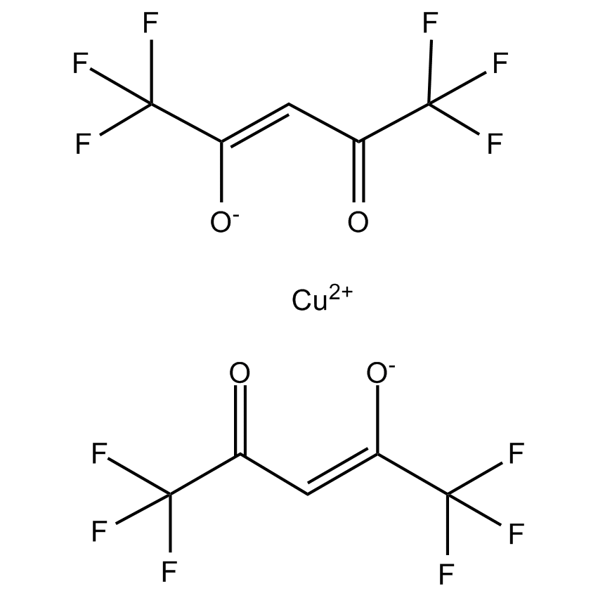
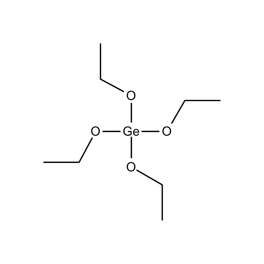
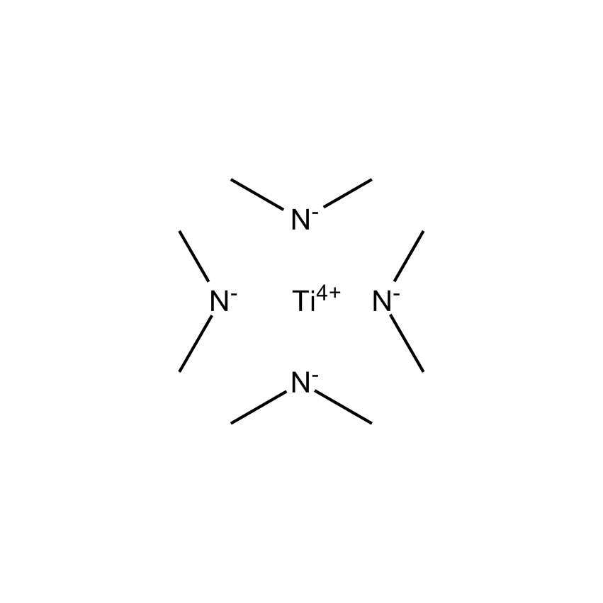
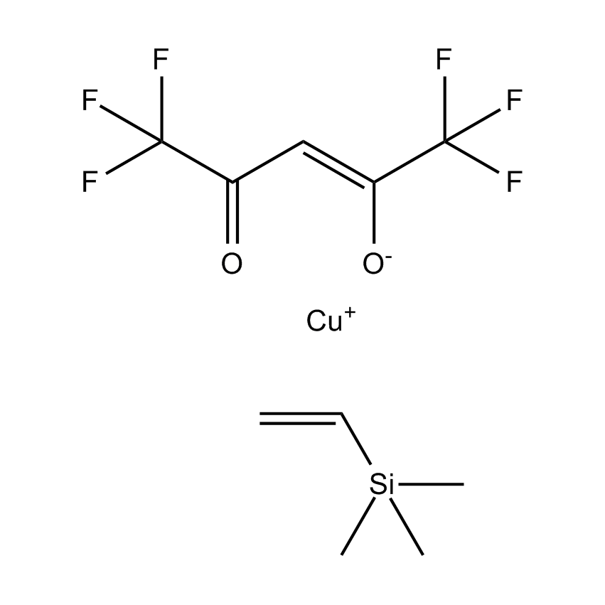
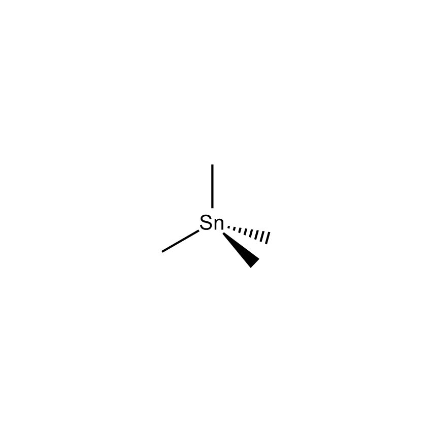
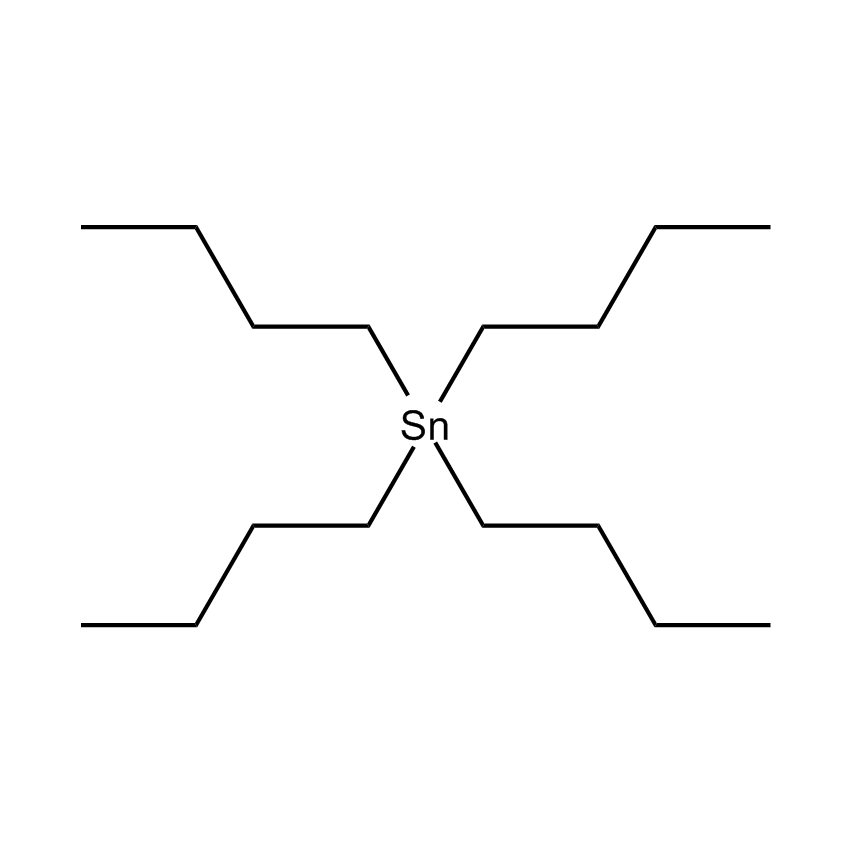
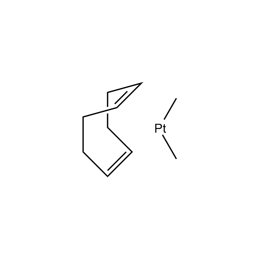
Using differing precursor and reactive gases allows films of varied composition to be made. SnO2, ZnO, and Pt films can be grown using the following precursors and reactants respectively: tetramethyltin and oxygen; diethylzinc and oxygen; and dimethylplatinum(II) cyclooctadiene ({COD}PtMe2) and hydrogen. Gelest offers a range of metal-organic precursors for CVD applications for microelectronics. Precursors are available for commonly employed metals, such as silicon, copper, aluminum, titanium, tantalum and tungsten. These precursors are volatile solids or liquids and can be used to deposit metal thin films in typical CVD or atomic layer deposition (ALD) processes. Typical applications are for metal interconnects or diffusion barriers. In addition, metal-organic precursors that are volatile and reactive in the gas phase are employed for CVD. A wide variety of co-reactants and reaction conditions can be used to deposit mainly metal, metal oxides or metal nitrides. As such, Gelest offers a product line of metal alkoxide, substituted diketonate, amide, alkyl and halogen complexes.
Uses
Microelectronic Device Fabrication
Optical Storage
CVD is the preferred method since it is well-established with good scalability, reproducibility, and uniformity. It is also capable of high rates and good composition control.
Electronic Storage
Atomic layer deposition (ALD) method is a specialized CVD technique that is useful for depositing thin films for microelectronic applications where the material must be deposited in trenches with high aspect ratios.
With you every step of the way
Gelest sales, customer service, technical support and regulatory experts are on-call, ready to help.
Have a question or need technical support?
Looking for quick answers to some common questions?

Need to do a surface coverage or starting ratio calculation?
Interested in our specialty packaging solutions?
Products
©Gelest Inc. 2026