


Materials used in photovoltaic devices are usually silicon (monocrystalline, polycrystalline or amorphous), gallium arsenide, metal chalcogenides and organometallics.
Organic solar cells have become a hot topic in industrial research as solution-processable conjugated organic materials have the potential to enable simple fabrication of low-cost, mechanically flexible, and large area photovoltaic devices that allow relevant access to the sun’s sustainable and clean energy. Significant effort has been devoted toward increasing the power conversion efficiency of such solar cells. A major breakthrough was achieved by using bulk hetero-junction structures, wherein the active layer is spin-coated from a mixed solution of donor and acceptor materials. The resulting partially demixed blend structure allows for efficient exciton ionization at the large interfacial area, while also maintaining adequate charge transport and extraction through bi-continuous donor and acceptor phases.
The organic solar cells are the only photovoltaic device that uses molecules to absorb photons and convert them to electric charges without the need of intermolecular transport or electronic excitation. It is also the only such solar cells that separate the two functions of light harvesting and charge-carrier transport, whereas conventional photovoltaic devices perform both operations simultaneously. This imposes stringent demands upon the optical and electronic properties of the semiconductor, i.e., its band gap and band position, as well as charge-carrier mobility and the recombination time of photogenerated charges, restricting greatly the choice of suitable materials that can act as efficient photovoltaic converters.
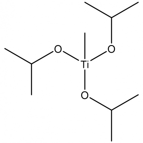
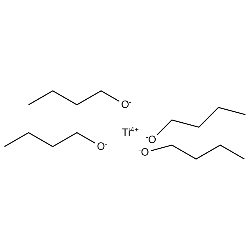
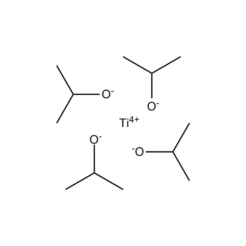
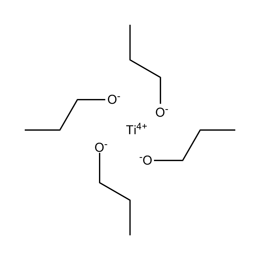
The molecular sensitizer or semiconductor quantum dot is placed at the interface between an electron (n) and hole (p) conducting material. The former is typically a wide band semiconductor oxide, such as TiO2, ZnO, or SnO2, while the latter is a redox electrolyte or a p-type semiconductor. Upon photoexcitation, the sensitizer injects an electron in the conduction band of the oxide and is regenerated by hole injection in the electrolyte or p-type conductor. Because the sensitizer injects electrons in the n-type and holes in the p-type collector, only majority carriers are generated. These charges move in their respective transport medium to the front and back contacts of the photocell, where they are collected as electric current. The electric field present in the vicinity of the junction separates the positive and negative charges generated under illumination, attracting the electrons to the n-doped and the holes to the p-doped material. To impart a sufficiently long lifetime to the photo-generated electron-hole pairs, the use of very pure materials is required. Gelest does work with companies to achieve higher purity levels when they are requested. The chemical purification of the semiconductor entails a high cost for the photovoltaic converter. Sunlight is harvested by the sensitizer that is attached to the surface of a large band gap semiconductor, typically a film constituted of titania nanoparticles.
A series of processes must occur efficiently in a good, ‘next-generation’ solar cell. These are:
- photon absorption by the active layer,
- exciton migration to, and charge transfer at the interface,
- separation of the charges from their mutual Coulomb attraction, and
- transport of separated charges to the electrodes.
Each of these processes can be monitored by optical spectroscopy, making it a powerful tool for measuring device performance. Optical probes are very valuable tools to study the nature of excited states and the dynamics of charge transfer and recombination processes in donor-acceptor systems. The excited states are generated by an excitation laser pulse, and their absorption is measured by recording the transmission of a second pulse. The second laser pulse arrives a controllable time after the excitation pulse.
Devices featuring new semiconductors will eventually come and decrease the production costs remarkably. To avoid charge carrier recombination inside the cell, exciton transportation pathways must be short and exciton separation has to be facilitated. Transferred to the device architecture, this means small domains of each donor or acceptor material and large interfacial areas in between them – both of which can be accomplished by controlling the cell design on the nanoscale. Further understanding of the charge recombination processes and especially their dependence on nanoscale morphologies is required to push efficiencies further, to extend the high efficiencies to larger area devices, and to reduce the reliance on trial and error for structure and device optimization. Gelest materials are helping to develop such structure-property-morphology correlations.
Organic–inorganic lead halide-based perovskites solar cells are by far the highest efficiency solution-processed solar cells, threatening to challenge both DSC, thin film and polycrystalline silicon ones. Perovskite solar cells with transparent contacts may be used to compensate for the thermal losses of silicon solar cells in tandem devices, offering a way to overcome efficiency limitations in other types of solar cells. However, perovskite top cells in tandem structures require contact layers with high electrical conductivity and optimal transparency. Despite the intense research in this area, concerns surrounding the long-term stability as well as the toxicity of lead in the archetypal perovskite, CH3NH3PbI3, have been raised. Although the search for lead-free perovskites has naturally shifted to other transition metal cations and formulations that replace the organic moiety, efficiencies with these substitutions are still substantially lower than those of the lead-based perovskite. The perovskite family offers rich multitudes of crystal structures and substituents with the potential to uncover new and exciting photophysical phenomena that hold the promise of higher solar cell efficiencies. As the search for new materials similar to CH3NH3PbI3 continues, Gelest does offer to custom synthesize and scale up a metal organic derivative that you exclusively need to make the next generation of the hybrid perovskite solar cells. In this regard we stand behind our mission statement: “to enable your technology.”
Uses
Mesoscopic solar cells
Recently, mesoscopic solar cells have made an impact in commercial markets. DSC (dye sensitized solar cells) and perovskite solar cells (refer to the end of this application note) have over the last 10 years seen commercialization and performance growth (some have now had 20 years of outdoor use with >100 million cycles). Gelest, Inc. offers a variety of precursors for the various types of solar cells as well as for anti-reflection and surface modification coatings.
Organic solar cells
Organic solar cells have become a hot topic in industrial research as solution-processable conjugated organic materials have the potential to enable simple fabrication of low-cost, mechanically flexible, and large area photovoltaic devices that allow relevant access to the sun’s sustainable and clean energy.
Organic–inorganic lead halide-based perovskites solar cells
Perovskite solar cells
With you every step of the way
Gelest sales, customer service, technical support and regulatory experts are on-call, ready to help.
Have a question or need technical support?
Looking for quick answers to some common questions?

Need to do a surface coverage or starting ratio calculation?
Interested in our specialty packaging solutions?
Products
©Gelest Inc. 2026