Silane Building Blocks enabling 21st Century Innovation
From artificial intelligence to next-generation diagnostics, many of today’s most advanced technologies depend on precise control at the molecular and surface level. Silane chemistry plays a critical—often unseen—role in enabling these innovations.
Structurally analogous to organic compounds, silanes are built around a tetravalent silicon atom that can be functionalized with a wide range of reactive groups. This versatility enables the design of tailored molecules through reactions such as halogenation, alkoxylation, and amination—bridging inorganic materials with organic functionality.
Once synthesized, silanes are used to modify surfaces and control interfacial behavior. In semiconductor manufacturing, techniques such as Atomic Layer Deposition (ALD) and Chemical Vapor Deposition (CVD) enable precise, layer-by-layer construction at the nanoscale. In life science applications, silanes form single-molecule monolayers that can be further functionalized for enzyme immobilization and biosensing—providing durable, covalent bonding under demanding conditions.
At Gelest, silane development is guided by application requirements—not just molecular design. Our capabilities in chlorosilane chemistry, purification, analytical characterization, and custom synthesis enable us to deliver materials that meet the performance and consistency demands of advanced technologies. By operating at the intersection of research and production, we collaborate closely with customers to accelerate iteration on molecular design and impurity control, helping shorten development cycles and move more efficiently from lab-scale evaluation to commercial implementation.
As technologies scale and biological and electronic systems become more integrated, tighter control at the interface is the key driver for performance and reliability.
Market Highlights
Semiconductor & Advanced Electronics Manufacturing
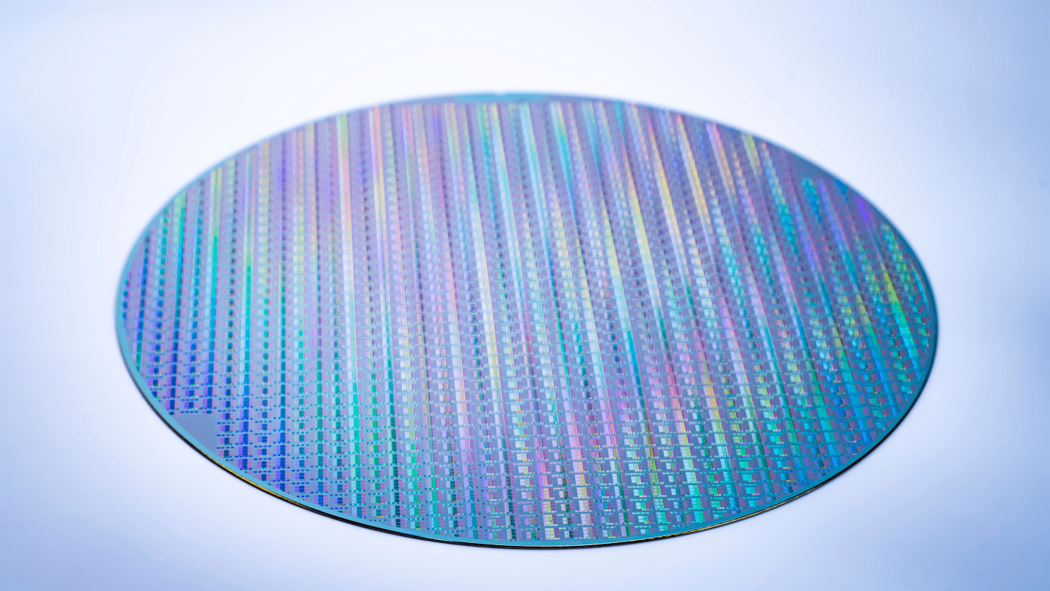
Engineering Surfaces at the Atomic Scale
The continued scaling of device architectures, coupled with increasing performance demands driven in part by artificial intelligence, makes atomic-scale control essential. Silanes play a foundational role in enabling the next generation of deposition processes used to build advanced semiconductor devices.
Functional silane precursors are widely used in techniques such as Atomic Layer Deposition (ALD) and Chemical Vapor Deposition (CVD), enabling conformal thin films with angstrom-level precision. These processes are critical for advanced logic and memory devices, where high-aspect-ratio features, complex 3D architectures, and heterogeneous integration require exceptional uniformity and interface control.
Beyond traditional dielectric and barrier layers, tailored silane chemistries are increasingly used to modify surfaces, improve adhesion between dissimilar materials, and enhance reliability in advanced packaging schemes such as chiplets and 3D stacking.
With continued scaling to smaller nodes and more complex integration, engineering surfaces at the molecular level has become a key lever for yield, performance, and long-term device stability.
Medical Device & Healthcare Technologies
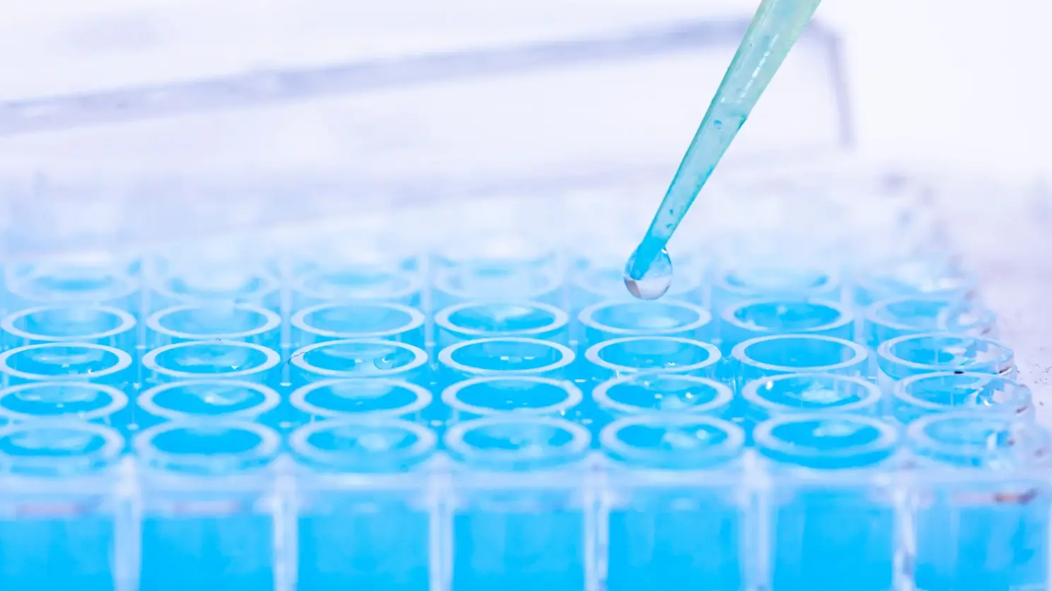
Controlling Surface Chemistry for Biological Function
In life science applications, silane chemistry enables precise control over biological interfaces—supporting performance improvements in diagnostics and pharmaceutical processing.
Silanes are commonly used to functionalize surfaces for immobilizing biomolecules such as enzymes, antibodies, and nucleic acids. By forming stable covalent linkages to substrates including glass, silica, and metal oxides, they create controlled environments that preserve biological activity while improving sensitivity, specificity, and reproducibility.
These capabilities are critical in advanced diagnostic platforms, including point-of-care systems where reliable biomarker detection depends on consistent surface chemistry.
In pharmaceutical manufacturing, silanes also enable purification and separation processes. Functionalized silica materials are widely used in chromatography to isolate complex biomolecules, including peptide-based therapeutics such as semaglutide.
As biologics continue to grow in importance, the ability to design selective and durable stationary phases becomes increasingly valuable for improving yield, purity, and process efficiency.
Aerospace, Space, & Defense
Controlling Surface Chemistry in Multi-Material Systems
Aerospace and defense systems increasingly rely on complex material stacks—metals, composites, coatings, and optical components—where performance is governed by interactions at material interfaces.
Silane chemistry enables precise modification of surface functionality, allowing interfaces to be tuned for compatibility, reactivity, and long-term stability. By introducing targeted functional groups, silanes bridge inorganic substrates with organic systems, enabling more controlled interactions in multi-material assemblies.
These capabilities are particularly valuable for:
- Controlled surface energy for improved wetting and coating uniformity
- Designed reactivity for bonding or functionalization
- Stable surface modification without altering bulk properties
Greater system complexity makes precise surface chemistry control essential for consistent performance.
Energy

Enabling Advanced Materials Through Controlled Chemistry and Purity
Energy technologies—from nuclear systems to electrification and emerging infrastructure—are pushing materials to perform under increasingly demanding thermal, chemical, and electrical conditions. In these environments, performance is often defined during material formation and at critical interfaces.
Silane chemistry provides a versatile platform for both surface modification and advanced material synthesis, particularly where precise control over composition and structure is required.
In many systems, purity is not just a specification—it is a key performance driver, directly influencing reliability and long-term stability.
Silanes support:
- High-purity material formation
- Improved consistency in critical processes
- Enhanced interfacial stability in multi-material systems
As next-generation energy technologies evolve, the value of precisely engineered, high-purity chemistries continue to increase.
Technical Spotlight
Aminosilanes for Next-generation Semiconductors
Aminosilanes — organosilicon compounds defined by Si–N bonds to dialkylamino or alkylamino groups — have become one of the most strategically important precursor families in advanced microelectronics. From silicon oxide and silicon nitride ALD to spacer films and gap-fill dielectrics, aminosilanes deliver a combination of volatility, tunable reactivity, and clean ligand chemistry that halide-based alternatives struggle to match.
Linear aminosilanes are open-chain molecules where one or more amino groups sit on a silicon center. Mono- and bis(amino)silanes are highly reactive and well suited to low-temperature growth on oxide and nitride surfaces. Tris- and tetrakis(amino) variants pack more ligands around the silicon, improving thermal stability and extending the usable ALD window. Cyclic azasilanes close the Si–N motif into a ring. The strained ring opens cleanly when it meets a surface –OH or –NH site, attaching in a single, byproduct-free step — making these molecules a strong fit for surface priming, functionalization, and inhibitor chemistries where clean, self-terminating attachment matters more than bulk film growth.
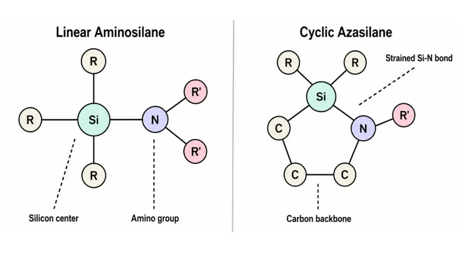
Together, the two families give process engineers a flexible toolkit: one class for building films, another for shaping where they grow. As architectures move to 3D stacks and sub-3 nm features, that flexibility is no longer optional — and aminosilane chemistry, halide-free and sterically tunable, is well positioned to deliver it.
Application Highlight
Area Selective Deposition – Extending Inhibition Beyond SiO₂
Area-selective atomic layer deposition (AS-ALD) takes a fundamentally different approach compared to conventional patterning. Rather than depositing a film everywhere and removing unwanted material later, it deposits material only where needed. Growth is confined to target regions—referred to as growth surfaces—while inhibitor molecules are often used to suppress precursor interaction with adjacent non-growth surfaces.
DMA-TMS (tris(dimethylamino)silane), one of the most widely studied aminosilane inhibitors, often fails to suppress nucleation on non-silica oxides such as Al₂O₃, HfO₂, and WOₓ—limiting selectivity on heterogeneous device stacks. Tailored silane structure extends inhibition beyond SiO₂ to these technologically relevant oxides. Graph 1 shows a clear performance hierarchy on HfO₂, with Inhibitor #2 outperforming Inhibitor #1, and both exceeding the performance of DMA-TMS relative to a SiO₂ reference deposition process. These results show that silane structure selection directly controls which oxide surfaces are inhibited—a practical requirement for AS-ALD on real, heterogeneous device architectures. The same molecular tunability that drives film growth also defines where it doesn’t—and that’s increasingly where the value lies.
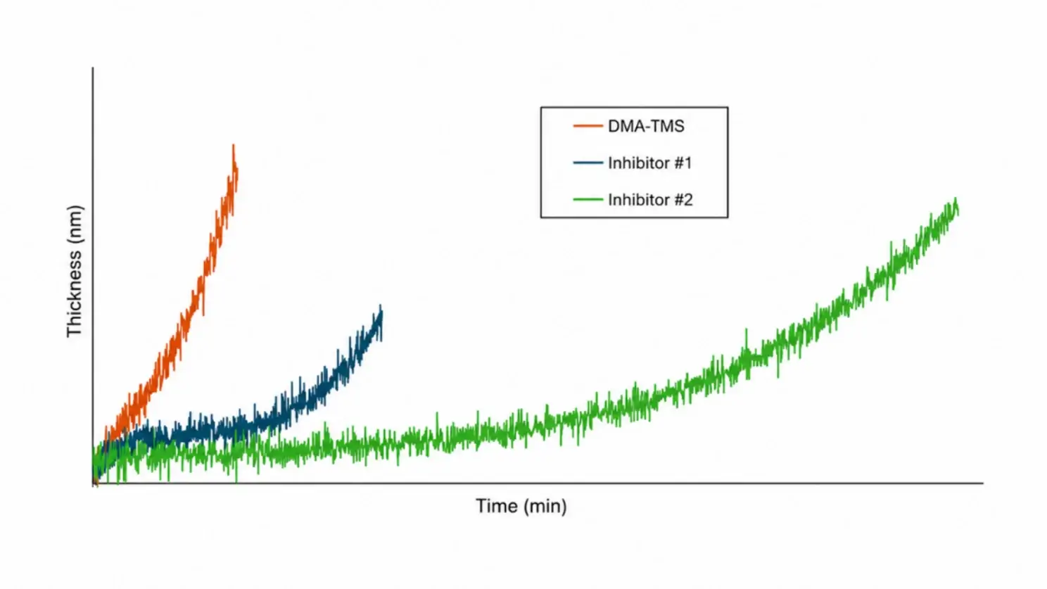
Graph 1. Inhibition performance of TDMAS, Inhibitor #1, and Inhibitor #2 on HfO₂ relative to a SiO₂ reference
Looking Ahead
Enabling Innovation at the Interface
Advancing technologies—from semiconductor architectures to next-generation diagnostics—are placing increasing emphasis on molecular-level control. In many cases, performance is defined not by bulk properties alone, but by interactions at material interfaces.
Silanes provide a versatile platform for engineering these interactions, enabling improvements in device performance, reliability, and functionality across diverse applications.
Whether enabling nanoscale deposition or stabilizing complex biological environments, silane chemistry plays a central role in modern material design.
At Gelest, we work closely with customers to translate these capabilities into practical solutions—combining silane design, custom synthesis, and analytical expertise to accelerate development and move innovations from concept to commercialization.
Upcoming Events
Connect with our technical team at the following industry events to discuss materials innovation, application challenges, and performance-driven solutions across our core markets:

- 9 – 11 June 2026
- Nuremberg, Germany
- Visit us at booth #6-111

- 28 June – 01 July 2026
- Tampa, Florida USA
- Visit us at poster AS-TuP007: Inhibition of Hafnia and Alumina using Silanes

- 2 – 4 September 2026
- Taipei, Taiwan
- Visit us at booth #L0900