More “Moore” Requires More Chemistry
For decades, semiconductor advancement has been driven largely by shrinking transistor dimensions. But as features approach atomic scales, quantum effects, heat generation, and increasingly complex device architectures are making continued scaling far more challenging.
Increasingly, the breakthroughs needed to move semiconductor technology forward are happening at the molecular and interfacial level.
Chemistry is being asked to deliver greater performance with fewer contaminants, enable smaller features and thinner films, address environmental concerns, and support increasingly complex material interfaces, all without sacrificing yield.
Five chemistry challenges are becoming particularly important:
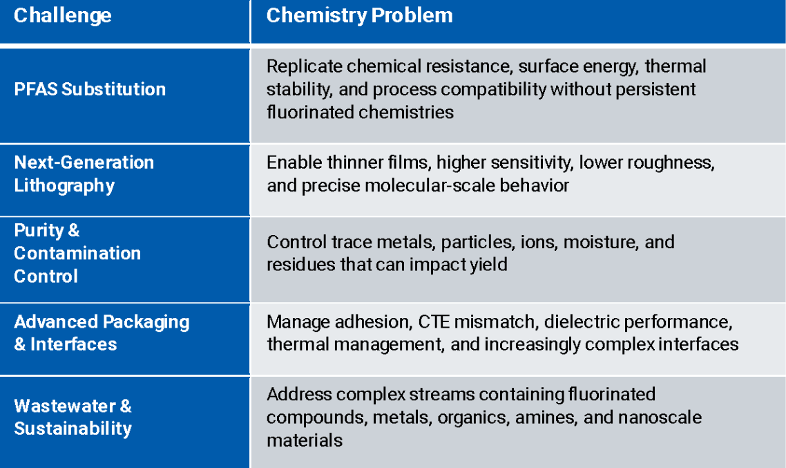
These challenges illustrate how materials chemistry is becoming increasingly important to the future of semiconductor manufacturing.
1. PFAS Substitution: Replicating Performance with New Chemistry
PFAS materials have historically provided a difficult-to-replicate combination of chemical resistance, thermal stability, low surface energy, and process performance. A 2026 American Chemical Society review concluded that complete PFAS elimination in semiconductor manufacturing is not presently feasible because of the breadth of applications and the complexity of qualifying alternatives.
Replacement efforts are progressing, but substitution is unlikely to occur uniformly across semiconductor manufacturing. Fluorine-free lithography materials are advancing, for example, while some dry-etch applications remain significantly more difficult to replace.
The challenge, therefore, isn’t simply to remove fluorine. It is a molecular-engineering challenge: identifying the performance that fluorinated chemistry provides and developing new materials capable of reproducing those critical properties.
2. Next-Generation Lithography: Printing the Nearly Impossible
High-NA EUV (High Numerical Aperture Extreme Ultraviolet) lithography represents an important step toward increasingly fine semiconductor patterning. As dimensions continue to shrink, however, conventional photoresists face a difficult tradeoff among resolution, sensitivity, and line-edge roughness.
These challenges are compounded by stochastic effects, random events at the molecular and atomic scale that can create defects when printing extremely small features.

Metal-oxide resists are receiving significant attention because their higher EUV absorption and etch resistance may offer advantages for advanced patterning. At the same time, deposition chemistry and other new materials approaches are being explored to enable future generations of lithography.
Solving these challenges will require increasingly precise control over molecular structure, material composition, purity, and interfacial behavior.
3. Purity & Contamination Control: When Parts per Billion Matter
As device dimensions shrink, contaminants that were once insignificant can become yield-limiting defects.
Different impurities create different challenges in the fab:
- Trace metals can introduce electrical defects.
- Particles can create pattern defects.
- Mobile ions can affect device reliability.
- Moisture can cause deposition and process variation.
- Residual organics can contaminate critical surfaces.
Even extremely small variations in molecular composition can matter. Chemically similar impurities or isomers may be difficult to detect and separate yet still affect downstream semiconductor processes. The potential consequences are significant: in 2019, faulty photoresist contributed to the loss of hundreds of millions of dollars in wafers at a leading semiconductor manufacturer.
As photoresists and deposition processes become more sensitive, controlling the surrounding environment also becomes increasingly important. Molecular contaminants in the air, for example, can interfere with chemically sensitive processes even when particulate contamination is well controlled.
Just as importantly, product purity and delivered purity are not necessarily the same thing.
Purity must be controlled throughout the material lifecycle, from raw materials and synthesis through purification, packaging, scale-up, and delivery. For some applications, maintaining purity through specialized containers or customer-owned cylinder fleets may be just as important as achieving purity during synthesis.
For semiconductor materials, purity isn’t simply a specification on a certificate of analysis. It is a supply-chain and process-control capability.
4. Advanced Packaging & Interfaces: More Interfaces, More Chemistry
AI accelerators and high-performance computing increasingly depend not only on transistor scaling, but also on chiplets, heterogeneous integration, 2.5D and 3D structures, hybrid bonding, and increasingly complex interconnect architectures.
Every additional layer and material creates another interface: silicon–dielectric, metal–polymer, adhesive–substrate, and many others.
These interfaces introduce challenges involving:
- adhesion and surface preparation
- coefficient-of-thermal-expansion (CTE) mismatch
- mechanical stress
- moisture protection
- dielectric performance
- thermal management
- long-term interfacial reliability

Surface modification, adhesion promotion, dielectric materials, thermal management, stress management, and interface engineering therefore become increasingly important as packaging architectures become more complex.
Specialty chemical companies with expertise in silanes, silicones, surface modification, and molecular design are well positioned to help materials developers engineer these increasingly demanding interfaces.
5. Wastewater & Sustainability: Solving the Challenges Chemistry Creates
Semiconductor wastewater is unusually complex because manufacturing streams can contain fluorinated compounds, metals, organic chemicals, amines, and nanoscale oxides.
PFAS compounds add another dimension to this challenge because of their environmental persistence. Although PFAS may be present at relatively low concentrations within much larger and more complex waste streams, semiconductor fabs process enormous volumes of water, and fluorinated materials may ultimately appear in liquid, gaseous, and solid waste streams.
Future materials development therefore must increasingly consider not only how a chemistry performs during semiconductor manufacturing, but also what happens to that chemistry afterward.
Chemistry enables semiconductor manufacturing. Increasingly, new chemistry will also be needed to reduce its environmental footprint.
The Next Generation of Semiconductors Will Be Enabled by Chemistry
As semiconductor architectures become smaller, more complex, and more integrated, materials challenges increasingly move to the molecular and interfacial level.
Contamination must be controlled at unprecedented levels. New chemistries must balance performance with environmental considerations. Advanced lithography requires extraordinary precision in molecular behavior. Advanced packaging requires increasingly sophisticated control of adhesion, interfaces, thermal behavior, and dielectric performance.
For specialty materials developers such as Gelest, these challenges create opportunities to apply expertise in silicon-based chemistry, silanes, silicones, surface modification, high-purity materials, and custom synthesis to the next generation of semiconductor technologies.
The path beyond traditional scaling won’t depend on physics and equipment alone.
Increasingly, it will depend on chemistry.
Upcoming Events
Connect with our technical team at the following industry events to discuss silane portfolio and custom synthesis for your unique applications:

Webinar:
Rethinking Silicones: The Role of PDMS in Next-Generation Medical Devices
- Michael Czuczola, PhD, Gelest Inc.
- 21 October 2026
- 11:00 AM US/Eastern
- Registration link: https://webinar.connectmeinforma.com/event/register/JAut3t4B2Iz1Zo7s?partnerref=EXTGelestNewsletter